百科名片
ISBN:9787115155481 [十位:7115155488]
頁數:581 重約:0.771KG
定價:¥65.00
內容提要
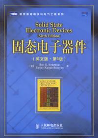
本書是介紹半導體器件工作原理的經典入門教材,其主要內容包括固體物理基礎和半導體器件物理兩大部分,同時也涵蓋半導體晶體結構與材料生長技術、積體電路原理與製造工藝以及光電子器件與高頻大功率器件等相關內容。
本書注重基本物理概念,強調理論聯繫實際,可作為高等院校電子信息類專業“固態器件與電路”專業基礎課的教材,也可供相關領域的研究人員和技術人員參考。
圖書目錄
1 CRYSTAL PROPERTIES AND GROWTH OF SEMICONDUCTORS
1.1 Semiconductor Materials
1.2 Crystal Lattices
1.2.1 Periodic Structures
1.2.2 Cubic Lattices
1.2.3 Planes and Directions
1.2.4 The Diamond Lattice
1.3 BulkCrystalGrowth
1.3.1 Starting Materials
1.3.2 Growth of Single-Crystal Ingots
1.3.3 Wafers
1.3.4 Doping
1.4 Epitaxial Growth
1.4.1 Lattice-Matching in Epitaxial Growth
1.4.2 Vapor-Phase Epitaxy
1.4.3 Molecular Beam Epitaxy
2 ATOMS AND ELECTRONS
2.1 Introduction to Physical Models
2.2 Experimental Observations
2.2.1 The Photoelectric Effect
Atom i Spectra
2.3 The Bohr Modlel
2.4 Quantum Mechanics
2.4.1 Probability and the Uncertainty Principle
2.4.2 The Schr6dinger Wave Equation
2.4.3 PotentialWellProblem
2.4.4 Tunneling
2.5 Atomic Structure and the Periodic lable
2.5.1 The Hydrogen Atom
2.5.2 The Periodic Table
3 ENERGY BANDS AND CHARGE CARRIERS IN SEMICONDUCTORS
3.1 Bonding Forces and Energy Bands in Solids
3.1.1 Bonding Forces in Solids
3.1.2 Energy Bands
3.1.3 Metals, Semiconductors, and Insulators
3.1.4 Direct and Indirect Semiconductors
3.1.5 Variation o! Energy Bands with AIIo Composition
3.2 Charge Carriers Semiconductors
3.2.1 Electrons and Holes
3.2.2 Effective Mass
3.2.3 Intrinsic Material
3.2.4 Extrinsic Material
3.2.5 Electrons and Holes in Quantum Wells
3.3 Carrier Concentrations
3.3.1 TheFermiLevel
3.3.2 Electron and Hole Concentrations at Equilibrium
3.3.3 Temperature Dependence of Carrier Concentrations
3.3.4 Compensation and Space Charge Neutrality
3.4 Drift of Carriers in Electric and Magnetic Fields
3.4.1 Conductivity and Mobility'
3.4.2 Drift and Resistance
3.4.3 Effects of lemperature and Doping on Mobility'
3.4.4 High-Field Effects
3.4 5 The Hall Effect
3.5 Invariance of the Fermi Level at Equilibrium
EXCESS CARRIERS IN SEMICONDUCTORS
4.1 Optical Absorption
4.2 Luminescence
4.2.1 Photoluminescence
4.2.2 Electroluminescence
4.3 Carrier Lifetime and Photoconductivity
4.3.1 Direct Recombination of Electrons and Holes
4.3.2 Indirect Recombination; Trapping
4.3.3 Steady State Carrier Generation; Quasi-Fermi Levels
4.3 4 Photoconductive Devices
4.4 Diffusion of Carriers
4.4.1 Diffusion Processes
4.4.2 Diffusion and Drift of Carriers; Built-in Fields
4.4.3 Diffusion and Recombination; The Continuity Equation
4.4.4 Steady State Carrier Injection; Diffusion Length
4.4.5 The Haynes-Shockley Experiment
4.4.6 Gradients in the Quasi-Fermi Levels
5 JUNCTIONS
5.1 Fabrication of p-n Junctions
5.1.1 Thermal Oxidation
5.1.2 Diffusion
5.1.3 Rapid Thermal Processing
5.1.4 Ion Implantation
5.1.5 Chemical Vapor Deposition (CVD)
5.1.6 Photolithography
5.1.7 Etching
5.1.8 Metallization
5.2 Equilibrium Conditions
5.2.1 The Contact Potential
5.2.2 Equilibrium Fermi Levels
5.2.3 Space Charge at a Junction
5.3 Forward-and Reverse-Biased Junctions;Steady State Conditions
5.3.1 Qualitative Description of Current Flow at a Junction
5.3.2 Carrier Injection
5.3.3 Reverse Bias
5.4 Reverse-Bias Breakdown
5.4.1 Zener Breakdown
5.4.2 Avalanche Breakdown
5.4.3 Rectifiers
5.4.4 The Breakdown Diode
5.5 Transient and A-C Conditions
5.5.1 Time Variation of Stored Charge
5.5.2 Reverse Recovery Transient
5.5.3 Switching Diodes
5.5.4 Capacitance of p-n junctions
5.5.5 The Varactor Diode
5.6 Deviations from the Simpl Theory
5.6.1 Effects of Contact Potential on Carrier Injection
5.6.2 Recombination and Generation in the Transition Region
5.6.3 Ohmic Losses
5.6.4 Graded Junctions
5.7 Metal-Semiconductor Junctions
5.7.1 Schottky Barriers
5.7.2 Rectifying Contacts
5.7.3 Ohmic Contacts
5.7.4 lypical Schottky Barriers
5.8 Heterojunctions
6 FIELD-EFFECT TRANSISTORS
6.1 Transistor Operation
6.1.1 The Load Line
6.1.2 Amplification a4d Switching
6.2 The Junction FET
6.2.1 Pinch-off and Saturation
6.2.2 Gate Control
6.2.3 Current-VoltageCharacteristics
6.3 The MetaI-SemiconductorFET
6.3.1 The GaAs MESFET
6.3.2 The High Electron Mobility Transistor (HEMT)
6.3.3 Short Channel Effects
6.4 The Metal-Insulator-Semiconductor FET
6.4.1 Basic Operation and Fabrication
6.4.2 The Ideal MOS Capacitor
6.4.3 Effects of Real Surfaces
6.4.4 ThresholdVoltage
6.4.5 MOS Capacitance-Voltage Analysis
6.4.6 Time-Dependent Capacitance Measurements
6.4.7 Current-Voltage Characteristics of MOS Gate Oxides
6.5 The MOSField-EffectTrans~stor
6.5.1 Output Characteristics
6.5.2 Transfer Characteristics
6.5.3 Mobility Models
6.5.4 Short Channel MOSFET I-V Characteristics
6.5.5 Control of Threshold Voltage
6.5.6 Substrate Bias Effects
6.5.7 Subthreshold Characteristics
6.5.8 Equivalent Circuit for the MOSFET
6.5.9 MOSFET Scaling and Hot Electron Effects
6.5.10 Drain-induced Barrier Lowering
6.5.11 Short Channel Effect and Narrow Width Effect
6.5.12 Gate-Induced Drain Leakage
7 BIPOLAR JUNCTION TRANSISTORS
7.1 Fundamentals o! BJT Operation
7.2 Amplification with BJTs
7.3 BJTFabrication
7.4 Minority Carrier Distributions and Terminal Currents
7.4.1 Solution of the Diffusion Equation in the Base Region
7.4.2 Evaluation of the Terminal Currents
7.4.3 Approximations of the Terminal Currents
7.4.4 Current Transfer Ratio
7.5 Generalized Biasing
7.5.1 The Coupled-Diode Model
7.5.2 Charge Control Analysis
7.6 Switching
7.6.1 Cutoff
7.6.2 Saturation
7.6.3 The Switching Cycle
7.6.4 Specifications for Switching Transistors
7.7 Other Important Effects
7.7.1 Drift in the Base Region
7.7.2 Base Narrowing
7.7.3 Avalanche Breakdown
7.7.4 Injection Level; Thermal Effects
7.7.5 Base Resistance and Emitter Crowding
7.7.6 GummeI-Poon Model
7.7 7 Kirk Effect
7.8 Frequency Limitations of Transistors
7.8.1 Capacitance and Charging Times
7.8.2 Transit Time Effects
7.8.3 Webster Effect
7.8.4 High-Frequency Transistors
7.9 Heterojunction polar Transistors
8 OPTOELECTRONIC DEVICES
8.1 Photodiodes
8.1.1 Current and Voltage in an Illuminated Junction
8.1.2 SolarCells
8.1.3 Photodetectors
8.1.4 Gain, Bandwidth, and Signal-to-Noise Ratio of Photodetectors
8.2 Light-Emitting Diodes
8.2.1 Light-Emitting Materials
8.2.2 Fiber-Optic Communications
8.3 Lasers
8.4 Semiconductor Lasers
8.4.1 Population Inversion at a Junction
8.4.2 Emission Spectra for p-n Junction Lasers
8.4.3 The Basic Semiconductor Laser
8.4.4 Heterojunction Lasers
8.4.5 Materials for Semiconductor Lasers
9 INTEGRATED CIRCUITS
9.1 Background
9.1.1 Advantages of Integration
9.1.2 Types of Integrated Circuits
9.2 Evolution oflntegrated Circuits
9.3 Monolithic Device Elements
9.3.1 CMOS Process Integration
9.3.2 Silicon-on-Insulator (SOl)
9.3.3 Integration of O.ther Circuit Elements
9.4 arge Transfer Devices
9.4.1 Dynamic Effects in MOS Capacitors
9.4.2 The Basic CCD
9.4.3 Improvements on the Basic Structure
9.4.4 App_lications of CCDs
9.5 Ultra LargeScalelntegration(ULSI)
9.5.1 Logic Devices
9.5.2 Semiconductor Memories
9.6 resting, Bonding, and Packaging
9.6.1 Testing
9.6.2 Wire Bonding
9.6.3 Flip-Chip Techniques
9.6.4 Packaging
1O HIGH-FREQuENCY AND HIGH-POWER DEVICES
10.1 Tunnel Diodes
10.1.1 Degenerate Semiconductors
10.2 The IMPATT Diode
10.3 The Gunn Diode
10.3.1 The Transferred-Electron Mechanism
10.3.2 Formation and Drift of Space Charge Domains
10.4 The p-n-p-n Diode
10.4.1 Basic Structure
10.4.2 The Two-Transistor Analogy
10.4.3 Variation of α with Injection
10.4.4 Forward-Blocking State
10.4.5 ConductingState 524
10.4.6 Triggering Mechanisms
10.5 The Semiconductor-Controlle rectifier
10.5.1 Turning off the SCR
10.6 Insulated-Gate Bipolar Transistor
APPENDICES
Ⅰ. Definitions of Commonly Used Symbols
Ⅱ. Physical Constants and Conversion Factors
Ⅲ. Properties of Semiconductor Materials
Ⅳ. Derivation of the Density of States in the Conduction Band
Ⅴ. Derivation of Fermi-Dirac Statistics
Ⅵ. Dry and Wet Thermal Oxide Thickness Grown on
Si(100) as a Function of Time and. lemperature
Ⅶ. Solid Solubilities of Impurities in
Ⅶ. Diffusivities of Dopants in Si and SiO2
Ⅸ. Projected Range and Straggle as Function of
Implant Energy in Si
ANSWERS TO SELECTED SELF QUIZ QUESTIONS
INDEX
作者介紹
Ben G.Streetman是美國國家工程院院士和美國藝術與科學院院士,IEEE會士和美國電化學學會(ECS)會士。現任美國德克薩斯大學奧斯汀分校工學院院長和該鷳電機工程與計算機工程講座教授,也是該校微電子研究中心的創始人和第一任主任(1984年-1996年)。Streetman教授的教學領域和研究興趣主要包括半導體材料與半導體器件兩個方面。


