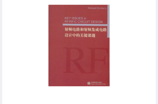
《射頻電路和射頻積體電路設計中的關鍵課題》是2005年高等教育出版社出版的圖書,作者是RichardChi-HsiLi。
基本介紹
- 作者:Richard Chi-Hsi Li
- ISBN:9787040159585
- 頁數:395
- 定價:40.10元
- 出版社:高等教育出版社
- 出版時間:2005-2
- 裝幀:簡裝本
內容介紹
作者介紹
作品目錄
1.1 Difference between RF and Digital Circuit Design
1.1.1 Case 1: Digital Circuits at Low Data Rate
1.1.2 Case 2: Digital Circuits at High Data Rate
1.2 Significance of Impedance Matching
1.2.1 Power Transportation from a Source to a Load
1.2.2 Maximizing of Power Transportation without Phase Shift
1.2.3 Conjugate Impedance Matching and Voltage Reflection Coefficient
1.2.4 Impedance Matching Networ
1.3 Problems due to Unmatched Status of Impedance
1.3.1 General Expression of Power Transportation
1.3.2 Power Instability and Additional Power Los
1.3.3 Additional Distortion and Quasi-Noise
1.3.4 Power Measurement
1.3.5 Power Transportation and Voltage Transportatio
1.3.6 Burning of a Transistor
References
Chapter 2 Impedance Matching
2.1 Impedance Measured by Small Signal
2.1.1 Impedance Measured by S Parameter Measurement
2.1.2 The Smith Chart: Impedance and Admittance Coordinatio
2.1.3 Accuracy of Smith Chartl
2.1.4 Relationship between the Impedance in Series and in Parallel
2.2 Impedance Measured by Large Signal
2.3 Impedance Matching
2.3.1 One Part Matching Network
2.3.2 Recognition of Regions in a Smith Chart
2.3.3 Two Parts Matching Network
2.3.4 Two Parts Upward and Downward Impedance Transformer
2.3.5 Three Parts Matching Network and Impedance Transformer
2.3.5.1 Topology Limitation of Two Parts Matching Network
2.3.5.2 Π Type Matching Network
2.3.5.3 T Type Matching Network
2.4 Some Useful Schemes for Impedance Matching
2.4.1 Designs and Tests when ZL is not 50 Ω
2.4.2 Conversion between“T” and “Π” Type Matching Network
2.4.3 Parts in a Matching Network
2.4.4 Impedance Matching between Power Transportation Units
2.4.5 Impedance Matching for a Mixer
References
Chapter 3 RF Grounding
3.1 A True Story
3.2 Three Components for RF Grounding
3.2.1 “Zero” Capacitors
3.2.2 Micro Strip Line
3.2.3 RF Cable
3.3 Examples of RF grounding
3.3.1 Test PCB
3.3.1.1 Small Test PCB
3.3.1.1.1 Basic Types of Test PCB
3.3.1.1.2 RF Grounding with a Rectngular Metallic Frame
3.3.1.1.3 An Example
3.3.1.2 Large Test PCB
3.3.1.2.1 RF Grounding by “Zero” Chip Capacitors
3.3.1.2.2 RF Grounding by a Runner or a Cable with Half or Quarter Wavelength
3.3.2 Isolation between Input and Output in a Mixer or an Up-converter
3.3.3 Calibration for Network Analyzer
3.4 RF Grounding for Reduction of Return Current Coupling
3.4.1 A Circuit Built by Discrete Parts on a PCB
3.4.2 RFICs
References
Chapter 4 Equivalent Circuits of Passive Chip Parts
4.1 Modeling of Passive Chip Parts
4.2 Characterizing of Passive Chip Parts by Network Analyzer
4.3 Extraction from the Measurement by Network Analyzer
4.3.1 Chip Capacitor
4.3.2 Chip Inductor
4.3.3 Chip Resistor
4.4 Summary
References
Chapter 5 Single-ended Stage and Differential Pair
5.1 Basic Single-ended Stage
5.1.1 General Description
5.1.2 Small Signal Model of a Bipolar Transistor
5.1.2.1 Impedance of a CE (Common Emitter) Device
5.1.2.2 Impedance of a CB (Common Base) Device
5.1.2.3 Impedance of a CC (Common Collector) Device
5.1.2.4 Comparison between CE, CB, and CC Device
5.1.3 Small-signal Model ofa MOSFET
5.1.3.1 Impedance of a CS (Common Source) Device
5.1.3.2 Impedance ofa CG (Common Gate) Device
5.1.3.3 Impedance of a CD (Common Drain) Device
5.1.3.4 Comparison between CS, CG, and CD Device
5.2 Differential Pair
5.2.1 DC Transfer Characteristic
5.2.1.1 DC Transfer Characteristic of a Bipolar Differential Pair
5.2.1.2 DC Transfer Characteristic of a CMOS Differential Pair
5.2.2 Small Signal Characteristic
5.2.3 Improvement of CMRR
5.2.4 Increase of Voltage Swing
5.2.5 Cancellation of Interference
5.2.6 Noise in a Differential Pair
5.3 Apparent Difference between Single-ended Stage and Differential Pair
5.4 DC Offset
5.4.1 DC Offset in a Single-ended Device
5.4.2 Zero DC Offset in a Pseudo-Differential Pair
5.4.3 Why "Zero" IF or Direct Conversion
5.4.4 DC Offset Cancellation
5.4.4.1 "Chopping" Mixer
5.4.4.2 DC Offset Calibration
5.4.4.3 Hardware Schemes
References
Chapter 6 Balun
6.1 Coaxial Cable Balun
6.2 Ring Micro Strip Line Balun
6.3 Transformer Balun
6.4 Transformer Balun Composed by Two Stacked 22 Transformers
6.5 LCBalun
References
Chapter 7 Tolerance Analysis
7.1 Importance of Tolerance Analysis
7.2 Fundamentals of Tolerance Analysis
7.2.1 Tolerance and Normal Distribution
7.2.2 6a, Cp, and Cp,
7.2.3 Yield Rate and DPU
7.2.4 Poisson Distribution
7.3 An Approach to 6a Design and Production
7.4 An Example: A Tunable Filter Design
7.4.1 Description of the Tunable Filter Design
7.4.2 Monte-Carlo Analysis
7.5 Appendix: Table of the Normal Distribution
References
Chapter 8 Prospect of RFIC Design269
Chapter 9 Noise, Gain, and Sensitivity of a Receiver317
Chapter 10 Non-linearity and Spurious Products339
Chapter 11 Cascaded Equations and System Analysis 358
Chapter 12 From Analog to Digital Communication System376

