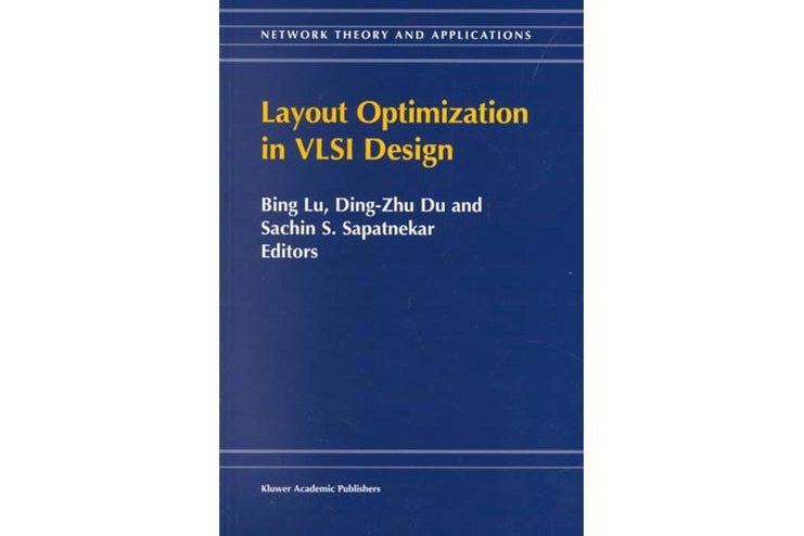
《Layout Optimization in VLSI Design》是2010年Springer; Softcover reprint of hardcover 1st ed. 2002 edition出版的圖書,作者是Bing Lu、Ding-Zhu Du、S. Sapatnekar。
基本介紹
- 外文名:Layout Optimization in VLSI Design
- 作者:Bing Lu、Ding-Zhu Du、S. Sapatnekar
- 出版社:Springer; Softcover reprint of hardcover 1st ed. 2002 edition
- ISBN:9781402000898
內容簡介,圖書目錄,
內容簡介
The exponential scaling of feature sizes in semiconductor technologies has side-effects on layout optimization, related to effects such as interconnect delay, noise, crosstalk, signal integrity, parasitics effects, and power dissipation, that invalidate the assumptions that form the basis of previous design methodologies and tools. This book is intended to sample the most important, contemporary, and advanced layout optimization problems emerging with the advent of very deep submicron technologies in semiconductor processing.
Audience: A reference work for graduate students, senior undergraduates, and researchers.
圖書目錄
Preface.
1. Integrated Floorplanning and Interconnect Planning; H.-M. Chen, et al.
2. Interconnect Planning; J. Cong.
3. Modern Standard-cell Placement Techniques; X. Yang, et al.
4. Non-Hanan Optimization for Global VLSI Interconnect; J. Hu, S.S. Sapatnekar.
5. Techniques for Timing-Driven Routing; J. Lillis.
6. Interconnect Modeling and Design with Consideration of Inductance; L. He.
7. Modeling and Characterization of IC Interconnects and Packagings for the Signal Integrity Verification on High-Performance VLSI Circuits; Y. Eo.
8. Tradeoffs in Digital Binary Adder Design: the Effects of Floorplanning, Number of Levels of Metals, and Supply Voltage on Performance and Area; V. Kantabutra, et al.
