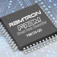
半導體存儲器主要包括揮發性存儲和非揮發性存儲兩大類。隨著消費類,攜帶型電子市場的發展,對半導體存儲器的需求越來越大。在市場的驅動下,半導體存儲器通過縮小單元尺寸提高存儲容量,降低單元成本,等比例縮小已成為半導體存儲技術發展的主要驅動力。
基本介紹
- 中文名:納米尺度新型半導體存儲器件研究
- 舉例:發性存儲和非揮發性存儲
- 技術:半導體存儲技術
- 分類:科技存儲項目
中文介紹
進一步,提出了基於體矽襯底的準SOI結構浮體DRAM單元,可在體矽襯底上製備,更適於嵌入式套用。與基於體矽襯底的傳統浮體DRAM單元相比,該新結構可以改善電流視窗和信號保持時間,此外,陣列中的單元可用共源共漏設計,單元面積從10F2縮小到6F2。在面向低功耗套用時,分析了帶帶隧穿編程方式在準SOI結構浮體DRAM單元的套用,結果表明相比於溝道熱電子機制,編程功耗可下降幾個數量級,同時電流視窗和保持時間基本相同。
對於非揮發性的快閃記憶體,分別針對快速讀取的NOR型快閃記憶體和高存儲密度的NAND快閃記憶體進行了相關研究。對於NOR型快閃記憶體,採用雙摻雜浮柵快閃記憶體(DDFG, Dual Dopoing Floating Gate)結構,開發了基於標準Foundry工藝的小尺寸DDFG快閃記憶體工藝。該結構可以提高熱電子編程的注入效率,降低編程功耗,提高單元保持特性。通過分析標準工藝小尺寸DDFG快閃記憶體工藝製備與大尺寸相比的一些特點,成功製備標準工藝下小尺寸DDFG快閃記憶體。實驗結果表明,小尺寸DDFG快閃記憶體仍具有編程效率提高、功耗下降的特性,而對小尺寸的工藝方案相較於大尺寸設計可靠性也得到了改善。通過測試分析,對工藝進一步最佳化,提出了一種大馬士革工藝方案。
針對提高快閃記憶體存儲密度及降低單元成本的要求,提出了一種三維圍柵薄膜電晶體(TFT,thin-film-transistor)NAND型快閃記憶體及其陣列架構,並設計開發了其工藝製備方案。所提出的三維結構工藝較為簡單,各層的主要工藝步驟可以同步完成,可以提高存儲密度,減小單元成本;快閃記憶體單元採用圍柵結構,可以提高TFT快閃記憶體的開關性能。通過工藝設計和對關鍵工藝步驟和參數最佳化,實驗製備出了三維圍柵TFT快閃記憶體單元及其NAND陣列結構,並測試了單元的開關、存儲特性和可靠性。測試結果表明圍柵TFT快閃記憶體相比於平面結構在電流開關比、亞閾斜率、遷移率、編程和擦除速度等方面都獲得較大改善,其中開關電流比達到1×10⁶,遷移率為平面結構20~30倍,單元導通電流達到了對體矽NAND快閃記憶體的要求。對三維圍柵TFT快閃記憶體單元的存儲特性的測試和分析表明在一定編程擦除條件,實現的圍柵TFT快閃記憶體單元具有較高的閾值視窗和可靠性。最後,設計了多級存儲的編程擦除條件,進一步論證了三維多級(MLC)NAND的存儲特性及可靠性。
關鍵字 無電容式DRAM,源漏能帶工程,浮柵快閃記憶體,薄膜電晶體快閃記憶體,三維快閃記憶體
英語介紹
The complicated capacitor process and reliability issue hinder 1T1C cell for embedded DRAM applications, while capacitor-less floating body DRAM cell (FBC) has attracted much attention. However, with the cell size scaling down, the performance of FBC is decreased, so a novel band-gap engineered source/drain floating body DRAM (BESD-FBDRAM) cell is proposed. The energy band offset with silicon - carbon source and drain can help to form a deeper potential well in the body region, which can effectively store more holes. Compared with normal FBC, BESD-FBDRAM can obtain 3 times larger signal window and 10 times longer retention time, while write speed keeps the same. In addition, BESD-FBDRAM cell exhibits more significant improvement for shorter channel devices, showing great potentials for further scaled generations. For bipolar FBC, a bipolar BESD-FBDRAM cell is proposed to increase the gate control window, reduce the drain voltage, and thus improve the cell reliability. Furthermore, for array applications, a source and drain underlap structure is also proposed to relieve the drain disturb of bipolar FBC.
To extend application fields of floating-body DRAM cell, a quasi-SOI structure floating-body DRAM based on bulk silicon substrate is proposed, which is more suitable for embedded DRAM applications. Compared with the bulk substrate floating-body DRAM cell, the quasi-SOI cell can achieve larger current window and longer retention time. Besides, the deep L-shape isolation enables common source/drain design for the adjacent quasi-SOI cell, and thus cell size is reduced from 10F2 in normal cell to 6F2. Moreover, a band-to-band tunneling programming method for low power consumption is also studied for quasi-SOI floating-body DRAM cell. The results show that compared to CHE (channel-hot-electron) programming method, the power consumption can be decreased by several orders of magnitude while the current window and hold time is almost the same.
Another issue is flash memory. For NOR flash memory, using a DDFG (Dual Doping Floating Gate) structure, we developed small size DDFG Flash memory process based on standard Foundry process. Due to an electron valley formed in the floating gate, this structure can improve flash cell retention characteristics. Through analysis of different features of DDFG flash memory based on standard Foundry process, we successfully fabricated 0.13um DDFG flash memory. The experimental results show that the small DDFG flash device can improve the programming efficiency and reduce power consumption. Moreover, a damascene process method was proposed to further optimize the DDFG device.
To continue enhance flash memory density, a three-dimensional gate-all-around (GAA) TFT NAND flash memory and its array architecture are proposed. The process flow of the proposed three-dimensional flash is relatively simple, as the memory cells of each layer can be formed synchronically, which can increase the storage density and reduce bit-cost. Then by process design and optimization, the three-dimensional TFT flash memory is demonstrated experimentally. Compared with the planar TFT flash cell, the GAA cell exhibited improved sub-threshold slope, carrier mobility and writing speed, which can overcome the difficulties for TFT applied to NAND flash memory. The measurement results show that the GAA TFT flash memory has a large memory window and good reliability characteristics. Finally, multi-level per cell (MLC) program/erase schemes are proposed and 3D MLC NAND flash is further demonstrated.
Key Words: floating body cell, band-gap engineered source/drain, floating gate flash, thin-film-transistor flash, three-dimensional flash

